Nanoscale tunneling microscopy goes contact-free
A new microscopy technique lets researchers characterize materials with incredible precision while keeping its distance — at least from a nanoscopic perspective.
Physicists from the University of Regensburg in Germany, the University of Manchester in England and Michigan State University developed the technique that enables observations at incredibly small sizes over ultrashort time scales. The invention, which could be used to investigate a variety of materials used in nanoscale science and engineering, was described in a paper on May 13 in the journal Nature Photonics.

“We are diversifying the technology so we can look at all the interesting materials we want to,” said Tyler Cocker, a Jerry Cowen Chair of Experimental Physics in the College of Natural Science at MSU.
The technique is a form of nanoscopy, which is akin to microscopy, but with much better resolution. This enables researchers to better characterize and implement materials being developed for emerging technologies, including quantum computers and next-generation solar cells.
For example, Cocker’s team at MSU is interested in exploring new materials for quantum computers as part of a five-institution collaboration supported by a recent $7.5 million grant from the Office of Naval Research.
“With our instrument, we can better determine what we have to worry about when designing a device, like what things will help it and what things will hurt it,” said Cocker, who is also an assistant professor in the Department of Physics and Astronomy.
The international team was led by Rupert Huber at the University of Regensburg in Germany, where Cocker also led a junior research team under Huber before joining MSU in 2018. In fact, the project has its roots in a proposal Huber and Cocker wrote together several years ago.
“It’s really nice having this come to fruition after all this development time,” Cocker said.
Also joining the effort were the teams of Jessica Boland, a functional materials and devices lecturer at the University of Manchester, and Jaroslav Fabian, a professor of physics with the Regensburg Center for Ultrafast Nanoscopy at the University of Regensburg.
To achieve high resolution in both space and time, the team’s work bridges two existing sets of micro- and nanoscopy techniques: one that uses light and another that works with a sample material’s electrons, Cocker said. In doing so, the researchers could see things in ways they hadn’t before — such as electrons moving between atomic layers in a material — and they could overcome limitations of the individual techniques.
For example, light microscopy comes with what’s known as the diffraction limit, which makes it challenging to get clear images of nanoscale objects or features. Existing microscopy techniques that use electrons offer better spatial resolution, but they typically work only if they’re in electrical contact with a sample.
“If you’re sample isn’t conducting, you’re out of luck,” Cocker said.
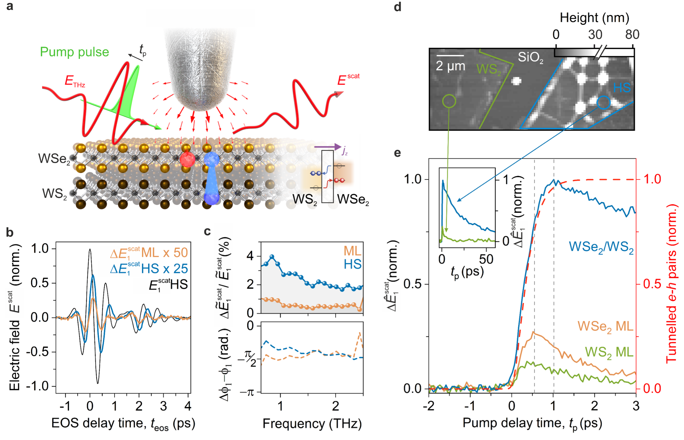
The new technique offers nearly atomic resolution without needing the electrical contact. Better still, the new method also achieves a time resolution as short as a quadrillionth of a second. By coupling extreme spatial and temporal resolution, the team can now record slow-motion movies of ultrafast electron dynamics on the nanoscale.
As far out as that may sound, the concept behind the technique works similarly to something that’s become pretty familiar. Contactless payment, which lets customers pay vendors using phones or credit cards, also exchanges information without making contact.
Huber, Cocker and their colleagues brought this idea down to the nanoscale using a sharp metallic tip that acts as a nano-antenna, which the researchers bring close to a sample. They then use a weak alternating electric field to scan the sample without making contact.
Instead of pulling banking information, however, these scans withdraw data about the sample’s physical properties. Also, the frequency used in the experiments is in the terahertz spectral range, approximately 100,000 times higher than what’s used in contactless payment scanners.
To demonstrate the technique, the team chose its first samples from a new material class called transition metal dichalcogenides. These materials feature atomically thin layers — useful for demonstrating the new technique’s resolution — and they’re also attractive candidates for next-generation solar cells.
With the new nanoscope, the researchers could watch how incoming light frees electrical charges within the material, which is crucial to a solar cell’s operation.
“We can’t wait to videotape further fascinating charge transfer processes in insulating, conducting and superconducting materials,” said Markus Plankl of the University of Regensburg, first author of the publication.
“Insights on the ultrafast transport on the relevant length and timescales will help us to understand how tunneling shapes the functionalities in a wide range of condensed matter systems,” added Plankl’s postdoctoral colleague and co-author Thomas Siday.
Although the new instrument lives in Germany, Cocker said this work dovetails nicely with his team’s work on MSU’s campus at the Ultrafast Terahertz Nanoscopy Laboratory.
“At MSU, we’re using complementary techniques,” Cocker said. “We think we can integrate those with the materials studied in this paper or go in a different direction, such as quantum computing. Developing these techniques gives us more avenues to explore materials that might be useful.”
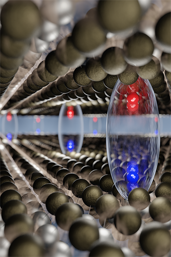
Banner image: An artistic representation of a material at the nanoscale shows two layers of gray orbs representing atoms at the top and bottom of the screen. Charged particles called electrons and holes — shown as red and blue spheres — move between these layers. Credit: Markus Plankl